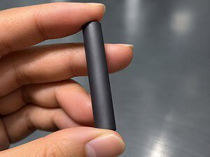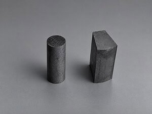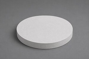
An InP boule cracks along its {110} cleavage plane the moment lateral force exceeds what the crystal can absorb. When that happens inside a wire cut, the result is not a slow degradation of quality — it is a scrap wafer. Edge chipping, hidden sub-surface cracks that only show up after lapping, or a full fracture that splits the ingot section before the cut completes. On an optical-grade indium phosphide boule, each of those outcomes writes off material that costs more per gram than most people realize until they have to replace it.
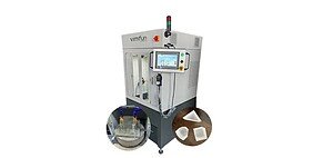
This application note covers how we approach indium phosphide cutting with endless electroplated diamond wire — the parameter window, the exit-end chipping control, and the limitations that still apply once everything is dialed in. For small-diameter boule sections and lab-scale wafer preparation, the SG20 platform is the starting machine reference; larger InP boules should be qualified on a larger-frame Vimfun system before production slicing. The target application is optical communication module manufacturing: InP wafers feeding photodetector and transceiver fabs where the cost of a scrapped substrate propagates all the way downstream.
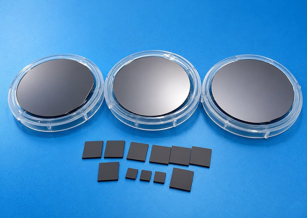
Why Indium Phosphide Wafers Fail at the Cutting Step
InP is in the awkward middle of the hardness ladder. It is softer than silicon and much softer than SiC, which sounds like it should make cutting easier. In practice it makes cutting harder, because the material does not resist the wire enough to produce a stable cut interface — the wire pushes into the crystal, and the crystal responds by cleaving instead of chipping away in micro-fragments the way a harder brittle material would.
The dominant failure mode is cleavage along the {110} family of planes. Zinc-blende structure, same as GaAs, same cleavage behavior. If the wire deflects laterally during the cut — because of tension drift, guide-wheel runout, or inconsistent feed force — the crack propagates along {110} rather than following the kerf path. The visible result on the finished wafer is edge chipping. The invisible result is sub-surface damage that only shows up when the lap/polish step removes the top layer and exposes the cracks underneath.
The second failure mode is end-of-cut chipping. When the wire approaches breakthrough at the exit face, the remaining unsupported crystal is thin, cantilevered, and under residual stress from the cut. Any vibration at that moment can split a corner off the wafer. On an InP wafer or wafer section destined for an optical communication fab, a visible edge chip is often enough to send the slice to reclaim.
Both failure modes are controllable, but the control has to happen at the cutting stage. Downstream grinding and polishing can clean up a cut face. They cannot repair a crack that has already propagated across a cleavage plane.
Endless Diamond Wire for Indium Phosphide Cutting
The cutting tool for this case is an endless electroplated diamond wire running as a closed loop. The wire is a nickel-electroplated bond holding diamond grit on a steel core. The loop runs around a drive wheel and a set of guide wheels, moving unidirectionally at constant speed — no reciprocation, no acceleration/deceleration cycles at the ends of each stroke.
The reason this geometry matters for indium phosphide cutting is not primarily cutting speed. It is force stability. A reciprocating wire reverses direction continuously, and every direction change is a moment where tension spikes and lateral force varies. On a material like silicon, the wafer tolerates it. On InP with its cleavage sensitivity, those tension spikes are exactly the perturbation that initiates a {110} crack.
A closed-loop wire holds a steady tension through the cut because it never stops. The drive wheel pulls one direction only; the guide wheels maintain the loop geometry; the wire delivers a constant linear velocity to the cut interface. From the crystal’s point of view, the cutting force profile is a slowly rising ramp rather than a continuous oscillation.
The electroplated bond is the right choice over resin-bonded wire here because of exposed grit height. Nickel-plated grit sits proud of the bond, which means the wire does mechanical cutting rather than rubbing. On a soft brittle material, rubbing generates heat and sub-surface damage. Cutting with exposed grit at the right speed generates chips and leaves the surface relatively undisturbed.
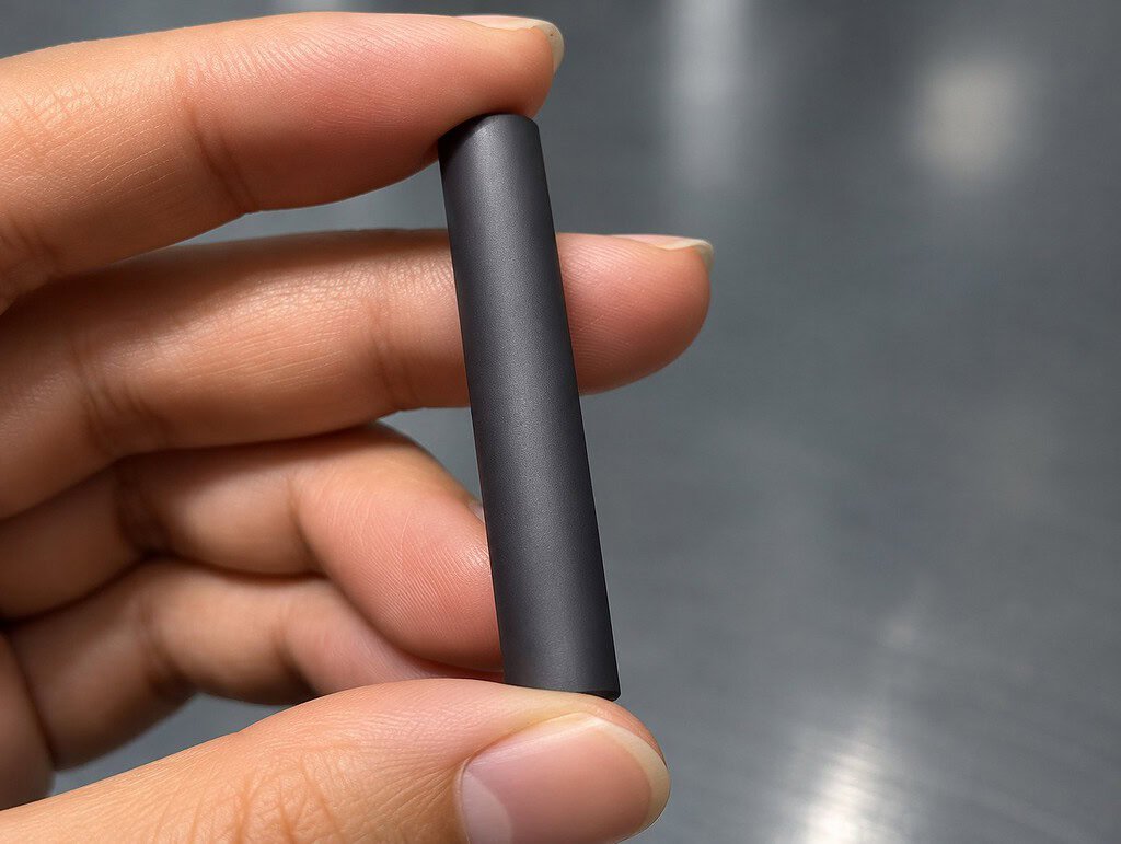
Process Parameters: Wire, Tension, Feed, Coolant
The parameter window below is what we start with for single-crystal InP boule sections on the SG20. It is a starting reference, not a universal recipe — crystal orientation, dopant type, boule diameter, and fixture stiffness all shift the optimum, and the final numbers need to be qualified on your material before production cuts begin.
- Wire diameter: 0.35–0.45 mm. The lower end minimizes kerf loss on expensive material; the upper end buys stiffness margin on larger-diameter boules where wire deflection becomes a concern.
- Wire speed: 30–45 m/s. Below 30 m/s the wire starts to grab rather than cut, which raises lateral force on the crystal. Above 45 m/s the thermal load at the cut interface rises faster than coolant can carry it away.
- Wire tension: 100–130 N. Low enough to avoid unnecessary stress on the wire joint and the guide-wheel bearings; high enough to resist the lateral deflection that initiates cleavage fracture. Tension stability through the cut matters more than the exact set point.
- Feed rate: 0.5–1.5 mm/min across the main body of the cut, with reductions at entry and exit (see next section). This is slower than you would run silicon on the same machine. InP cannot absorb aggressive feed.
- Coolant: White mineral oil for the primary case, or a neutral water-based coolant where oil contamination of downstream wet-chemistry is a concern. Delivery at both the wire entry and exit sides of the cut, with enough flow to flush InP swarf out of the kerf. Recirculated swarf is a scratch source on the finished wafer face.
The reasoning behind the wire-speed and tension interaction is covered in more depth in the wire speed, tension, and feed rate technical reference. For InP specifically, treat the three parameters as a coupled set — moving one requires re-checking the other two.
Exit-End Chipping Control: Sacrificial Backing and Dual-Speed Feed
The single most effective intervention we apply for InP cutting is a sacrificial backing plate at the exit end of the cut, combined with a reduced feed rate at both entry and exit segments.
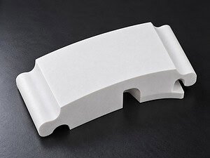
The sacrificial backing is a plate — typically a sintered ceramic or a dense graphite — mounted so that the wire breaks through from the boule into the backing material rather than into open air. The function is pure mechanical: the backing supports the thin, cantilevered edge of the wafer at the moment of breakthrough, so the remaining crystal cannot flex and split. The backing takes the chipping instead of the wafer.
The feed rate drop at entry and exit is layered on top of this. For the first 2–3 mm of the cut and the final 2–3 mm, feed is reduced to roughly half of the main-body rate. At entry, this prevents the initial contact shock that chips the top edge of the wafer. At exit, it reduces the force profile at breakthrough even with the backing in place.
Both measures are required. The backing without feed reduction still produces exit chipping because the breakthrough force spikes faster than the backing can distribute it. Feed reduction without the backing reduces the risk but does not eliminate it. Together they close the exit-end chipping failure mode to the point where it is no longer the dominant yield loss.
A note on operator practice: even with the backing and dual-speed feed in place, the exit segment still deserves attention. The feed profile is set in the machine controller, but boule-to-boule variation in end-face geometry can shift exactly when breakthrough occurs. Operators who manually verify the backing contact before each cut catch more exit-chipping issues than those who trust the controller alone.
Cutting Result and Downstream Readiness
The outcome from this parameter window on healthy boules is a wafer with a narrow kerf, low edge chipping, and low sub-surface damage — ready to enter the lap and polish sequence without additional edge trim.
Qualitatively: the kerf face has the matte-grey appearance characteristic of controlled diamond-wire cutting on compound semiconductors, with no visible fracture lines, no chip-outs at the edges, and no evidence of cleavage propagation into the wafer body. The sub-surface damage layer is shallow enough that the standard lap allowance removes it without over-thinning the wafer.
The point is that the wafer coming off the saw is ready for downstream processing without rework. For an optical communication module fab consuming InP substrates in volume, that is the metric that matters — not the as-cut dimensions in isolation, but the fraction of cut wafers that enter the lap process without an extra inspection-and-rework loop.
For production qualification, we normally record kerf width, edge-chip size, Ra, cycle time per cut, and post-lap defect rate on the customer’s actual boule material before locking the recipe. Those numbers matter more than a generic datasheet value because InP behavior changes with crystal orientation, dopant system, and incoming boule geometry.

Known Limitations and Recipe Qualification
Three limitations apply to this process that are worth stating directly:
Kerf width is wider than slurry-based reciprocating wire saws. An endless diamond wire at 0.35–0.45 mm diameter produces a wider kerf than a 0.14 mm slurry-wire multi-wire cut. If kerf-loss per wafer is the dominant cost driver — which it can be on very small, high-value InP boules — slurry-wire remains competitive. The trade-off we buy with endless diamond wire is cutting speed, cleanliness (no slurry handling), and lower sub-surface damage at a given feed rate.
Exit-end chipping risk is reduced, not eliminated. The sacrificial backing and dual-speed feed close most of the exit chipping failure mode, but a thin wafer breaking off an off-axis cut can still fracture asymmetrically. Operator vigilance at the exit segment remains part of the process.
The parameter window is a starting reference. The ranges above are what we use for single-crystal InP boule sections in a typical optical communication substrate configuration. Different crystal orientations (semi-insulating Fe-doped InP, S-doped n-type, Zn-doped p-type) respond differently to the same wire-speed and feed combination. Any production program should qualify the recipe against the specific crystal grade and orientation on representative material before committing production boules.
For teams approaching this process from an adjacent material — silicon ingot cutting or germanium slicing — the basic endless-wire process transfers directly, but the parameter set does not. InP is softer than silicon and more cleavage-prone than germanium, and both differences push the recipe toward lower feed, tighter tension control, and more aggressive exit protection than you would use on the sister materials.
FAQ
Q: Can we run InP and GaAs on the same wire without changing anything?
Both materials have the same zinc-blende cleavage behavior, and the machine configuration is portable. But the parameter set is not identical — GaAs tolerates slightly higher feed rates for the same chipping result, and the wire-wear profile is different because of the different hardness. Changing the material without re-qualifying the recipe will cost yield.
Q: Why not use a thinner wire to reduce kerf loss?
Below 0.30 mm the wire loses the stiffness needed to resist deflection on larger-diameter InP boule sections, and deflection is what initiates cleavage fracture on this material. For small sections (under 50 mm) a thinner wire can work; for larger sections, 0.35–0.45 mm is the more practical range.
Q: Does the SG20-R variant offer anything specific for InP?
The SG20-R shares the core architecture of the SG20. For a straight boule-slicing application like this one, the SG20 is the primary platform. SG20-R becomes relevant if your scope expands beyond parallel slicing — talk to us about the specific operation before specifying either.
Q: How reliable is this process after recipe qualification?
The process is stable within the parameter window above once the recipe is qualified on your specific crystal grade. The yield-limiting events are typically material-side (boule-to-boule variation in cleavage behavior, incoming boule geometry) rather than machine-side. Process monitoring at the cutting stage — first-article inspection on each ingot section — catches the material-side drift early enough to adjust.
If you are preparing InP wafers or compound-semiconductor samples and want to validate the cutting window before committing production material, send Vimfun the boule diameter, crystal orientation, dopant type, target wafer thickness, and downstream lapping allowance. We can recommend a first-pass wire, tension, feed, coolant, and backing setup for sample testing.