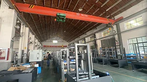
In semiconductor manufacturing, wafer preparation defines not only the material utilization but also the overall yield in downstream processes. As silicon, silicon carbide (SiC), and compound semiconductor devices scale in size and performance, traditional slicing methods face limitations in kerf loss, edge damage, and throughput. Endless diamond wire cutting (EDW), which employs a continuous diamond-coated wire loop, is emerging as a reliable and efficient technology for both ingot slicing and wafer resizing.

This article explores the technical principles of EDW, its advantages compared to conventional saws, and its role in improving efficiency and yield in semiconductor production.
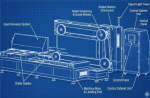
How Endless Diamond Wire Cutting Works
EDW relies on a continuous loop of diamond-coated wire, driven at high linear speed under controlled tension. Unlike reciprocating wire saws or internal-diameter blades, the endless loop ensures a steady cutting force and uniform motion, minimizing vibrations and thermal fluctuations.
Key operating parameters include:
- Wire speed: Typically up to 60–80 m/s for hard substrates.
- Tension: Controlled to prevent wire wander and maintain thickness uniformity.
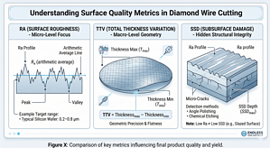
- Abrasive grain size: Fine diamonds minimize subsurface damage; coarser grains increase removal rate.
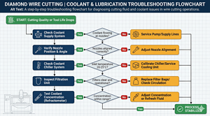
- Coolant and filtration: Critical to remove debris, reduce heat, and prevent contamination.
Technical Advantages in Semiconductor Manufacturing
1. Reduced Kerf Loss
Conventional ID saws or reciprocating systems produce wider kerf widths, leading to significant material loss. EDW can achieve kerf widths as narrow as 0.35–0.40 mm, directly increasing the number of wafers per ingot and lowering cost per wafer.
2. Lower Subsurface Damage (SSD)
With continuous cutting action, EDW reduces crack initiation and SSD depth, which in turn decreases the chemical mechanical polishing (CMP) removal budget. Less polishing time translates into lower consumable usage and higher throughput.
3. Edge Quality and Reliability
Wafer edges are prone to chipping, cracks, and micro-fractures. EDW’s steady mechanical load produces smoother edges, reducing edge-related die breakage during dicing or packaging. This directly improves die strength and final yield.
4. Compatibility with Hard and Brittle Materials
Materials such as SiC, GaN, and sapphire present unique challenges due to hardness and brittleness. EDW, combined with optimized coolant and abrasive specifications, provides stable slicing performance even in these demanding substrates.
Applications Across the Semiconductor Value Chain
Ingot Slicing
EDW is used to slice silicon and SiC boules into wafers with precise thickness and minimal material loss. For expensive materials like SiC, the economic benefits of kerf reduction are particularly significant.
Wafer Resizing and Coring
Research fabs and specialty shops often need wafers resized or cored to smaller diameters for pilot lines. EDW enables precise resizing, re-notching, and SEMI-standard edge compliance.
Edge Preparation
EDW can be integrated with edge beveling and rounding processes, ensuring wafers meet SEMI M1 specifications. Stronger and cleaner edges reduce defectivity in advanced packaging and thin wafer handling.
Post-Process Yield Improvement
By lowering SSD and improving edge strength, EDW reduces failures during downstream CMP, lithography, and dicing. This improves both line yield and overall equipment effectiveness (OEE).
Cost of Ownership Considerations
When evaluating new slicing technologies, fabs weigh both capital investment and operational cost. EDW offers:
- Material savings: More wafers per ingot due to narrower kerf.
- Consumable efficiency: Longer wire life compared to blades, and reduced CMP consumables.
- Throughput: Stable process with reduced rework and scrap.
- Yield impact: Fewer cracks, stronger edges, and lower defectivity.
For high-value materials like SiC, these factors combine to deliver a compelling cost-of-ownership advantage.
Case Example: SiC Wafer Processing
In a pilot evaluation, EDW was applied to 150 mm SiC wafers for resizing and edge preparation. Results showed:
- 35% reduction in edge chipping compared to mechanical coring.
- 10–15% lower CMP removal budget.
- 20% increase in average die strength.
- 1.5–2% gross yield improvement in pilot lots.
These results highlight EDW’s potential to scale from R&D labs to mass production.

Conclusion
Endless diamond wire cutting is more than an incremental improvement—it is a transformative technology for semiconductor wafering. By enabling finer kerfs, reducing subsurface damage, and improving edge quality, EDW helps fabs extract more value from each ingot while safeguarding downstream yield.
👉 To learn more about how endless diamond wire cutting systems can enhance semiconductor manufacturing, contact our team for detailed technical information and application guidance.