Einführung
Silicon wafers are at the heart of modern electronics, serving as the foundation for semiconductors, solar cells, and integrated circuits. As the demand for thinner, more precise, and defect-free wafers continues to rise, manufacturers are turning to advanced cutting methods to meet industry standards. One such innovation is the use of Diamantdraht. But can Diamantdraht effectively cut silicon wafers? The answer is a resounding yes — and here’s why.
为什么精度在硅晶圆切割中如此重要
Silicon is both hard and brittle, which makes it difficult to cut using traditional methods without causing micro-cracks, chipping, or material loss. Conventional blade sawing and slurry-based wire sawing often struggle to deliver the level of accuracy required in high-end semiconductor production.
This is where Diamantdraht comes in. With its exceptional hardness and wear resistance, Diamantdraht enables ultra-precise, low-damage slicing of silicon wafers, ensuring minimal kerf loss and superior surface quality.

Diamond Wire vs. Traditional Cutting Materials
To better understand the advantages of Diamantdraht, let’s compare it directly with conventional cutting materials such as steel wire or slurry wire.
| Comparison Factors | Diamantdraht | Traditional Cutting Materials |
|---|---|---|
| Präzision beim Schneiden | Extremely high; ideal for ultra-thin wafers | Moderate; prone to edge chipping and micro-cracks |
| Material Loss (Kerf Width) | Minimal kerf, maximizes silicon utilization | Wider kerf, leads to more material waste |
| Qualität der Oberfläche | Smooth surface finish; minimal need for post-processing | Rougher surfaces; requires additional polishing |
| Schneidgeschwindigkeit | Faster and more efficient | Slower and less productive |
| Sauberkeit | Clean process with minimal debris | Messier; more dust and slurry |
| Tool Wear & Durability | Lower wear; longer tool life | Higher maintenance and frequent replacements |
| Kompatibilität der Materialien | Suitable for hard materials like silicon, sapphire, SiC | Limited to basic materials |
| Cost Efficiency (Long Term) | Higher initial cost but better long-term savings | Lower upfront cost but higher operating expenses |
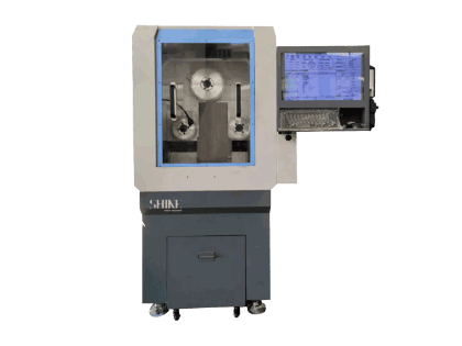
Working Principle of Diamond Wire
Diamond wire consists of a thin metal or resin-coated wire embedded with synthetic diamond particles. As the wire moves at high speed across the material surface, the diamond abrasives grind away the silicon with minimal mechanical stress. This process results in:
- Smoother surfaces with fewer micro-defects
- Reduced material loss due to a thinner kerf width
- Higher throughput thanks to faster cutting speeds
- Cleaner processing with less contamination and waste
For these reasons, Diamantdraht has become the go-to solution for slicing monocrystalline and polycrystalline silicon ingots in the photovoltaic and semiconductor industries.
Applications in the Semiconductor Industry
Diamond wire is widely used in:
- Solar panel manufacturing (cutting silicon ingots into wafers)
- IC chip production
- MEMS fabrication
- LED substrate slicing
As the industry moves toward smaller, more efficient components, the need for precise, low-damage cutting grows — and Diamantdraht is uniquely equipped to deliver.

Abschluss
So, can Diamantdraht cut silicon wafers? Absolutely. It offers unmatched precision, minimal material loss, and a cleaner, faster, and more efficient slicing process. As demand for high-performance semiconductors and solar cells continues to accelerate, Diamantdraht is emerging as the standard cutting solution for the future of silicon wafer processing.